A trusted manufacturer of high-end semiconductor packaging equipment, JAF provides innovative bonding solutions engineered to improve production efficiency, precision, and long-term reliability.
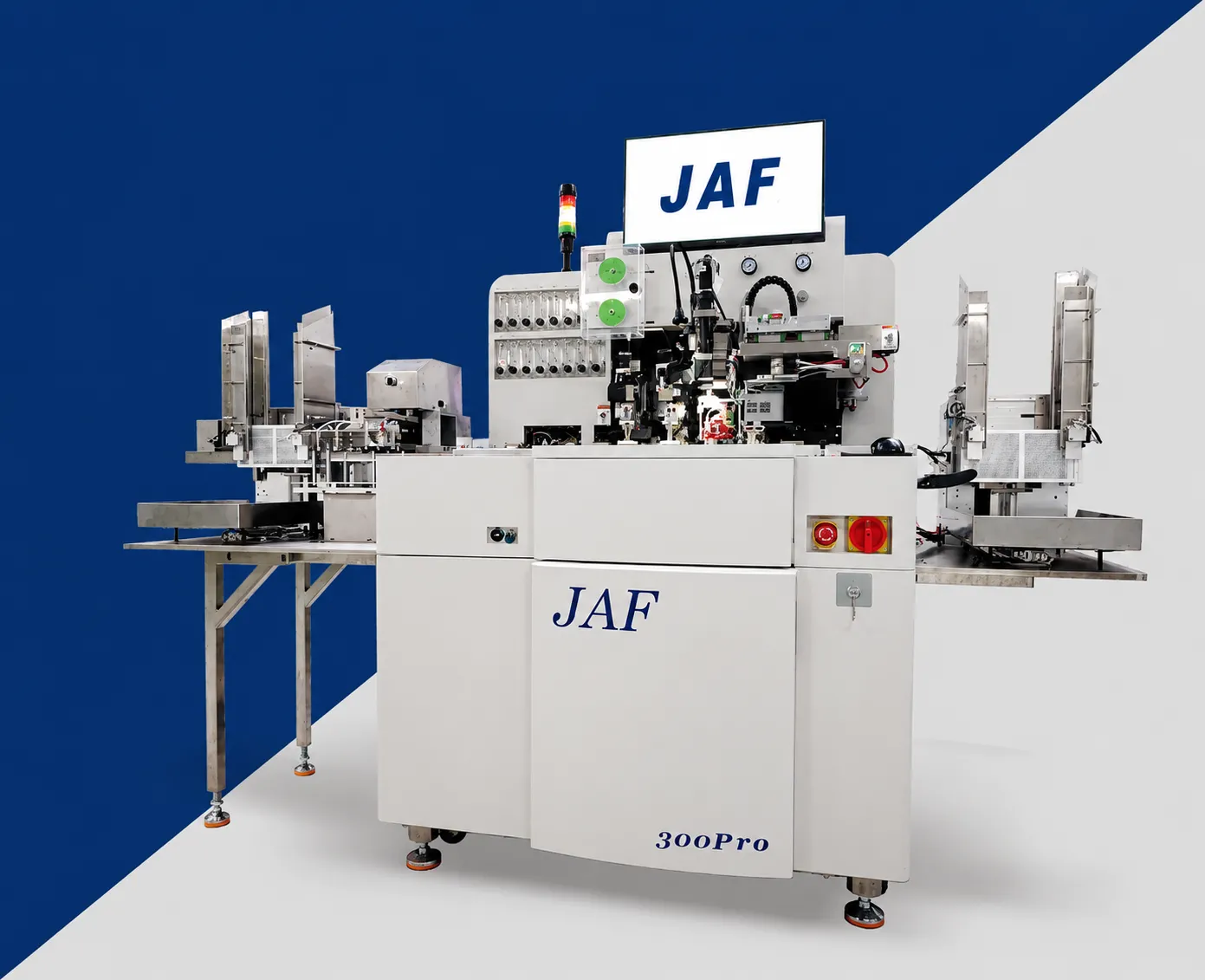
| Applications | TO series / PDFN series / TOLL series / IPM series, etc. |
| Die size | 0.8mm × 0.8mm – 12mm × 12mm |
| Die placement | ±50μm @3σ |
| Rotation | ±2° @3σ |
| Wafer size | 6″, 8″ |
| UPH | 3000 ~ 7000 |
| Void Rate | Single <2%, total <5% |
| BLT | 25μm–75μm |
| Die tilt | <35μm |
| Lead frame size | L: 170–300mm W: 25–70mm (90mm Optional) T: 0.3–2.8mm |
| Dimensions | 2048mm × 1300mm × 1650mm |
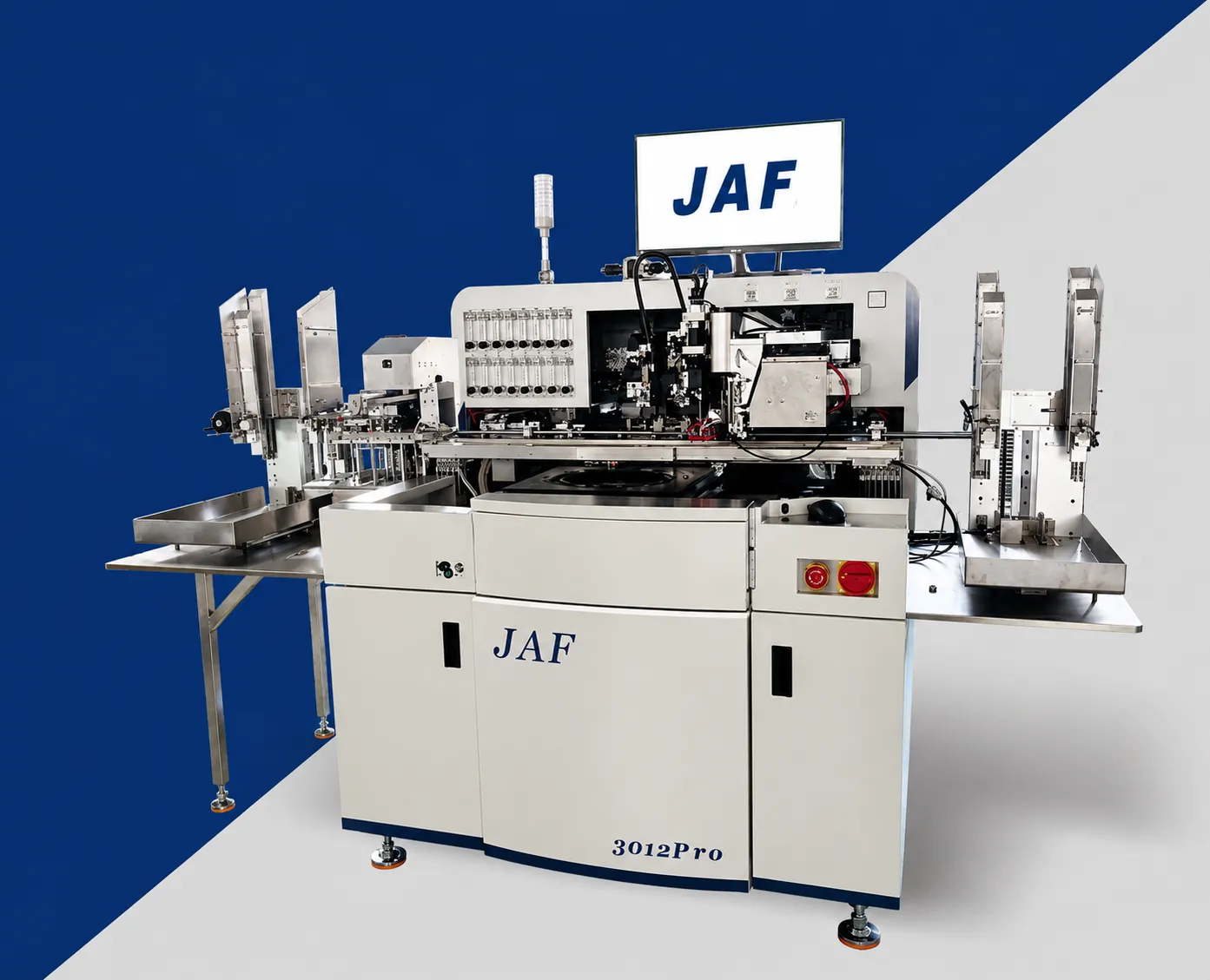
| Applications | TO / PDFN / TOLL / IPM series, etc. |
| Die size | 0.8mm × 0.8mm – 12mm × 12mm |
| Die placement | ±50μm @3σ |
| Rotation | ±2° @3σ |
| Wafer size | 6″, 8″, 12″ |
| UPH | 3000 ~ 7000 |
| Void Rate | Single <2%, total <5% |
| BLT | 25μm–75μm |
| Die tilt | <35μm |
| Lead frame size | L: 170–300mm W: 25–90mm (100mm optional) T: 0.3–2.8mm |
| Dimensions | 2230mm × 1420mm × 1650mm |
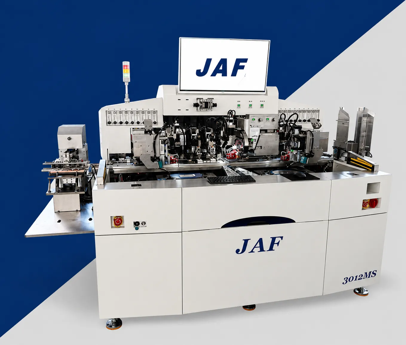
| Applications | TO / PDFN / TOLL / IPM series |
| Die Size | 0.8mm × 0.8mm – 12mm × 12mm |
| Die placement | ±50μm @3σ |
| Rotation | ±2° @3σ |
| Wafer size | 6″, 8″, 12″ |
| UPH | 2000–4000 (depending on product) |
| Void Rate | Single <2%, total <5% |
| BLT | 25μm–75μm |
| Die tilt | <35μm |
| Lead frame size | L: 170–300mm W: 25–90mm T: 0.3–2.8mm |
| Dimensions | 2830mm × 1465mm × 1565mm |
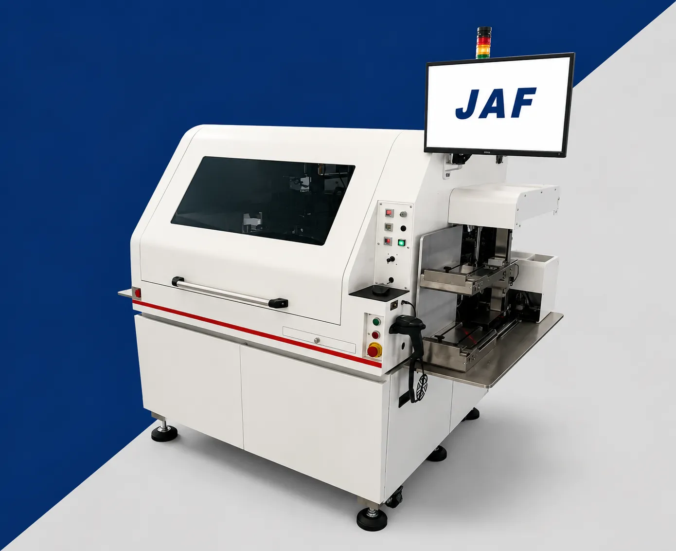
| Applications | Package: SOP, SSOP, TSOP, LQFP, TSSOP, SOT, QFN, PDFN, LFPAK, SOD, SMA, SMB, SMC, TOLL, TO, IPM series. |
| Die placement | Standard XY: ±25μm @3σ Theta: Die size ≥ 2 × 2 mm ±1° @3σ Die size < 2 × 2 mm ±2° @3σ Uplook |
| UPH | >12K for epoxy bonding (8+ rows lead frame) |
| Wafer Size | 6″, 8″, 12″ |
| Die Size | Die size: 0.25 × 0.25mm ~ 10 × 10mm; Thickness ≥0.06mm |
| Lead frame size | Lead frame: L:140 ~ 300mm W:30 ~ 102mm (below 30mm change rail) Thickness: 0.1 ~ 1.0mm |
| Bond force | 50~350gf (programmable) |
| Bond head | Bond Head Rotation: ±180°, height measurement uses Encoder feedback |
| Visual | Pre-Bond / Post-Bond / Post-Epoxy |
| Dimensions | 1400mm × 1400mm × 1600mm (Combine lead frame loading +500mm, unloading module +350mm) |
| Weight | 1800Kg |
| Software | 1. Windows with friendly operation interface, operation permission control. 2. Wafer Mapping function, and consumable-life management functions. 3. Real time working process display, Log information is saved in real time. 4. It supports standard SECS/GEM protocols. |
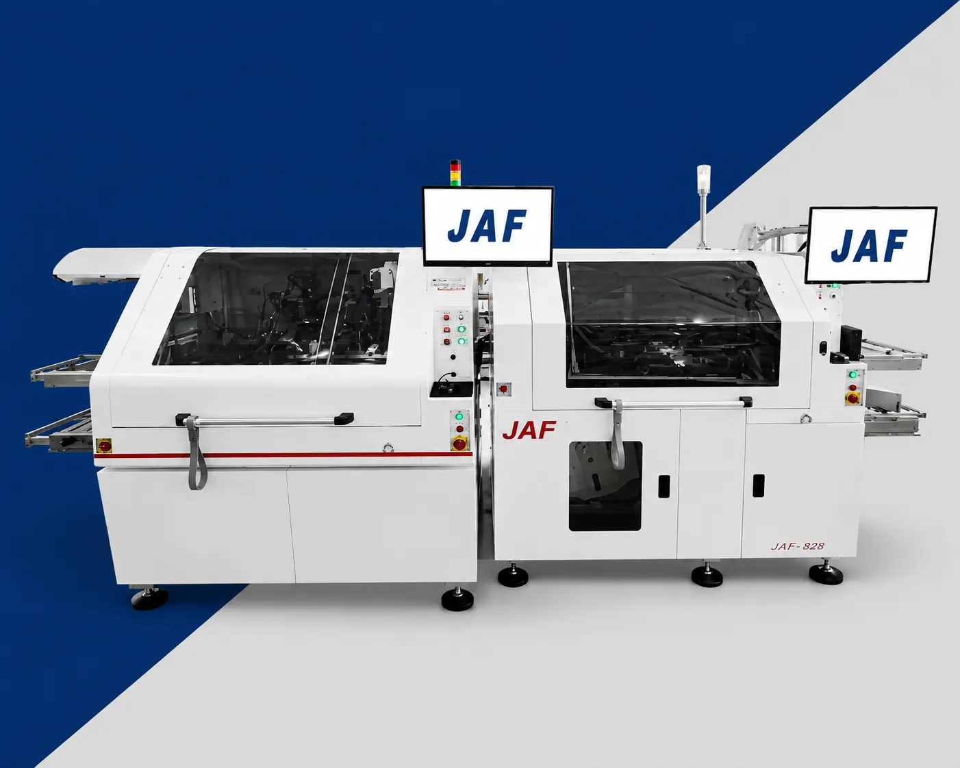
| Applications | Package: PQFN, DFN, LFPAK, SOD, SMA, SMB, SMC, TOLL, TO series etc. |
| Placement | Before: ±50μm, ±3° @3σ After: ±100μm, ±5° @3σ |
| UPH | Dual-dispense: >10K (8+ rows lead frame) 4-dispense: >14K (8+ rows lead frame) |
| Dispensing accuracy | The single dot dispensing diameter uniformity is ±15%, single dot dispensing ±50μm @3σ (Glue properties) |
| Clip min-cutting size | Clip >0.7mm, Clip thickness 0.1–0.4mm |
| Lead Frame | L: 140–300mm W: 30–100mm T: 0.1–1mm |
| Bond force | 300–1000gf, 1000–3000gf |
| Bond head | Bond Head Rotation: 180° |
| Singulation tool | Dimension (Width): ±0.05mm Vertical Burr <0.025mm Horizontal Burr <0.04mm |
| Visual | Pre-Bond / Post-Bond / Post-Epoxy |
| Dimensions | 1500mm × 1200mm × 1600mm (additional unloading mechanism +350mm) |
| Weight | 1800Kg |
| Software | 1. Windows with friendly operation interface, operation permission control. 2. Consumable life management functions. 3. Real-time working process display. Log information is saved in real time. 4. It supports standard SECS/GEM protocols. |
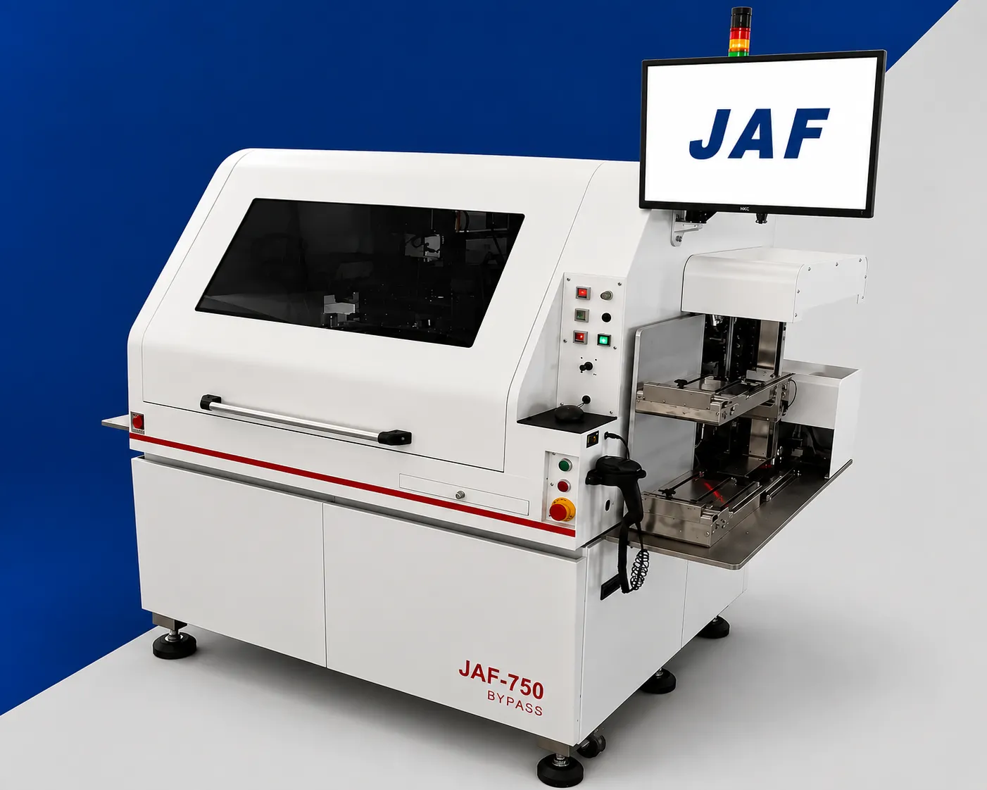
| Applications | DIP, SOP, SSOP, SIP, TSOP, PQFP, LQFP, TSSOP, SOT, QFN, DFN, QFP etc. |
| Die placement | X/Y: ±20μm @3σ Die size: >2×2mm ±1° @3σ Die size: <2×2mm ±2° @3σ |
| UPH | >16K (8+ rows lead frame) |
| Wafer size | 6″, 8″, 12″ |
| Die Size | Die size: 0.25×0.25mm–15×15mm; Die thickness ≥0.05mm; |
| Lead frame size | L:120–300mm W:30–100mm T:0.1–1.0mm |
| Bond force | 50–350gf programmable (Max 1000gf optional) |
| Bond head | Bond Head Rotation: ±180°, height measurement uses Encoder feedback |
| DAF function | Single-stage heating; Max temperature: 200±5° |
| Visual | Pre-Epoxy/Bond Post-Epoxy/Bond; Bridging Check / Epoxy Coverage Check |
| Function | 1. Four levels of operation permissions; each level can be set independently. 2. The equipment supports L/F Mapping and Wafer Mapping functions. 3. It supports standard SECS/GEM protocols and has Strip map and CIM parameter control functions. |
| Dimensions | L: 2280mm W: 1430mm H: 1600mm |
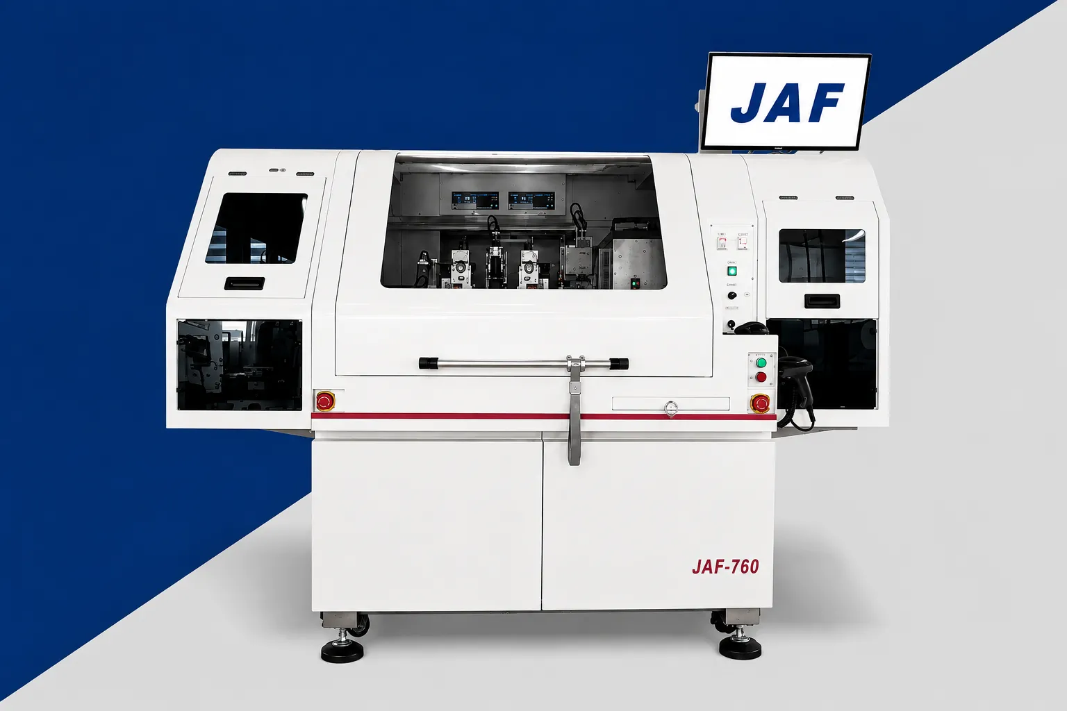
| Applications | SOT, SOP, SOIC, DFN, QFN, LQFP, PDFN, MEMS, LGA, etc. |
| Die placement | Standard X/Y: ±20μm @3σ Theta: ±2° @3σ UP LOOK X/Y: ±15μm @3σ Theta: ±1° @3σ |
| UPH | >13.5K (8+ rows lead frame) |
| Wafer size | 6″, 8″, 12″ |
| Die Size | Die: 0.25×0.25mm–15×15mm; Die thickness ≥0.05mm; |
| Lead frame size | Lead frame: L:120–300mm W:30–100mm T:0.1–1.0mm |
| Bond force | 30–350gf programmable (Max 2500gf optional) |
| Bond head | Bond Head Rotation: ±180°, height measurement uses Encoder feedback |
| DAF function | Three-stage heating; Max temperature: 200±5° |
| Visual | Pre-Epoxy/Bond Post-Epoxy/Bond; Bridging Check / Epoxy Coverage Check |
| Function | 1. Four levels of operation permissions; each level can be set independently. 2. Support L/F Mapping, Wafer Mapping function, standard SECS/GEM protocols. 3. Support and has Strip map and CIM parameter control functions. |
| Dimensions | L: 2280mm W: 1430mm H: 1600mm |
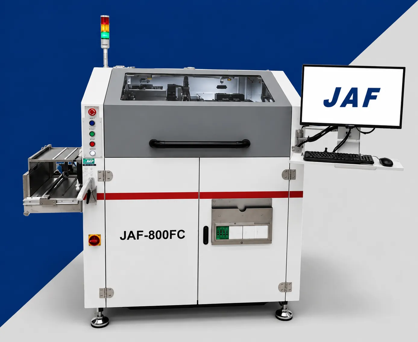
| Die Placement | XY ±10μm @3σ Theta |
| UPH | >5.5K, MAX: 6.5K |
| Material – Wafer | Wafer size: 8″, 12″ Die size: 0.4mm × 0.4mm ~ 10mm × 10mm Die thickness: 0.1mm ~ 3mm |
| Material – Substrate | Length: 110mm ~ 300mm Width: 30mm ~ 130mm Thickness: 0.1mm ~ 5mm Support LeadFrame Support jig carrier |
| Material – Magazine | Length: 120mm ~ 310mm Width: 35mm ~ 140mm Height: 70mm ~ 153mm |
| Bond force | 30~3000gf (programmable); 30~100gf: precision ±5g; 100~300gf: precision ±5%; 300~3000gf: precision ±10% |
| Bond head | Bond Head Rotation: ±180°, height measurement uses Encoder feedback |
| Visual | Pre-Bond / Pre Pick, Post-Bond, Down Look, Uplook |
| Software | Windows OS, graphical human-computer interaction interface, simple and user-friendly. Supports standard SECS/GEM protocols, extends Substrate/Strip/Wafer Mapping E142 functions. Supports Pseudo X-Ray, post-operation accuracy detection and other functions. |
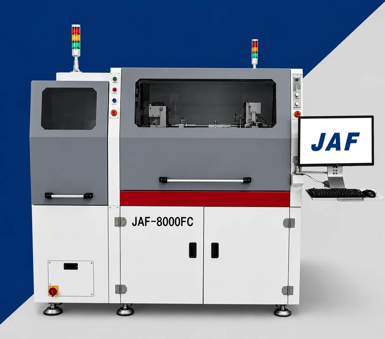
| Die Placement | XY ±5μm @3σ Theta |
| UPH | MAX: 8K |
| Material – Wafer | Wafer size: 8″, 12″ Die size: 0.5mm × 0.5mm ~ 30mm × 30mm Die thickness: 0.08mm ~ 3mm |
| Material – Substrate | L: 100–300mm W: 30–200mm Thickness: 0.1–3mm |
| Dipping | Max 30mm × 30mm, depth customized |
| Bond force | 30–3000gf (programmable); 30–200gf: precision ±10g; 200–3000gf: precision ±5% |
| Bond head | Bond Head Rotation: ±180°, height measurement uses Encoder feedback |
| Visual | Pre-Bond / Pre Pick, Post-Bond, Uplook |
| Software | Windows OS, graphical human-computer interaction interface, simple and user-friendly. Supports standard SECS/GEM protocols, extends Substrate/Strip/Wafer Mapping E142 functions. Supports Pseudo X-Ray, Post-bond precision detection. |
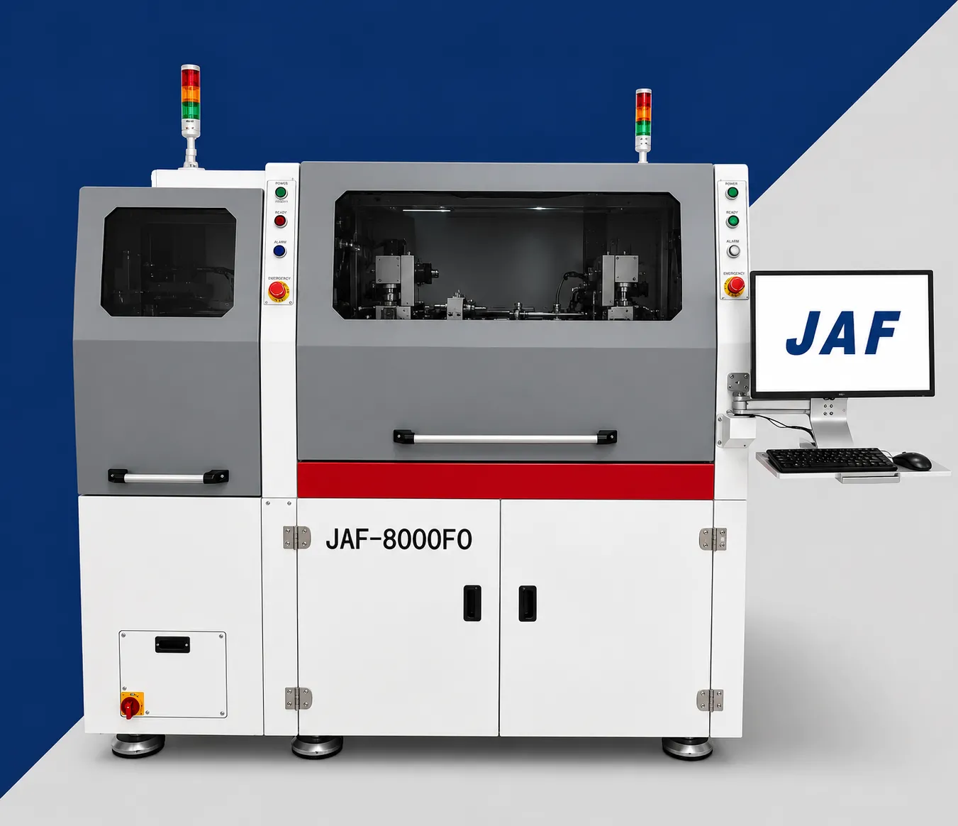
| Die Placement | XY ±5μm @3σ regional, 8μm @3σ global Theta |
| UPH | MAX: 8K |
| Material – Wafer | Wafer size: 6″, 8″, 12″ Die size: 0.5mm × 0.5mm ~ 30mm × 30mm Die thickness: 0.08mm ~ 3mm |
| Material – Substrate | Compatible 8″ / 12″ |
| C2W | 12″ carrier (300mm / 330mm FO-WLP carrier) |
| Bond force | 30~3000gf (programmable); 30~200gf: precision ±10gf; 200~3000gf: precision ±5% |
| Bond head | Bond Head Rotation: ±180°, height measurement uses Encoder feedback |
| Visual | Pre-Bond / Pre Pick, Post-Bond, Uplook |
| Software | Windows OS, graphical human-computer interaction interface, simple and user-friendly. Supports standard SECS/GEM protocols, extends Substrate/Strip/Wafer Mapping E142 functions. Supports Pseudo X-Ray, Post-bond precision detection. |
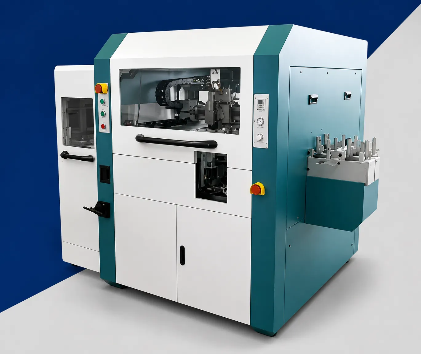
| Die placement | XY ±15μm @3σ Theta |
| UPH | MAX: 3K |
| Materials – Wafer | Wafer size: 6″, 8″, 12″ Die size: 1mm × 1mm ~ 15mm × 15mm Die thickness: 0.08mm ~ 3mm |
| Materials – Substrate | 465mm × 330mm |
| Materials – Waffle | 4″, 2 sets most (optional) |
| Materials – Preform | 2mm ~ 14mm, 3 sets most (optional) |
| Materials – Feeder | 2 sets most (optional) |
| Bond force | 30~300gf (programmable); Precision ±10g; |
| Bond head | 6 bonding heads (Bond force control), 360° rotation |
| Visual | Pre-Bond / Pre Pick, Post-Bond, Uplook |
| Software | Windows OS, graphical human-computer interaction interface, simple and user-friendly. Supports standard SECS/GEM protocols, extends Substrate/Strip/Wafer Mapping E142 functions. Supports Pseudo X-Ray, post-operation accuracy detection and other functions. |
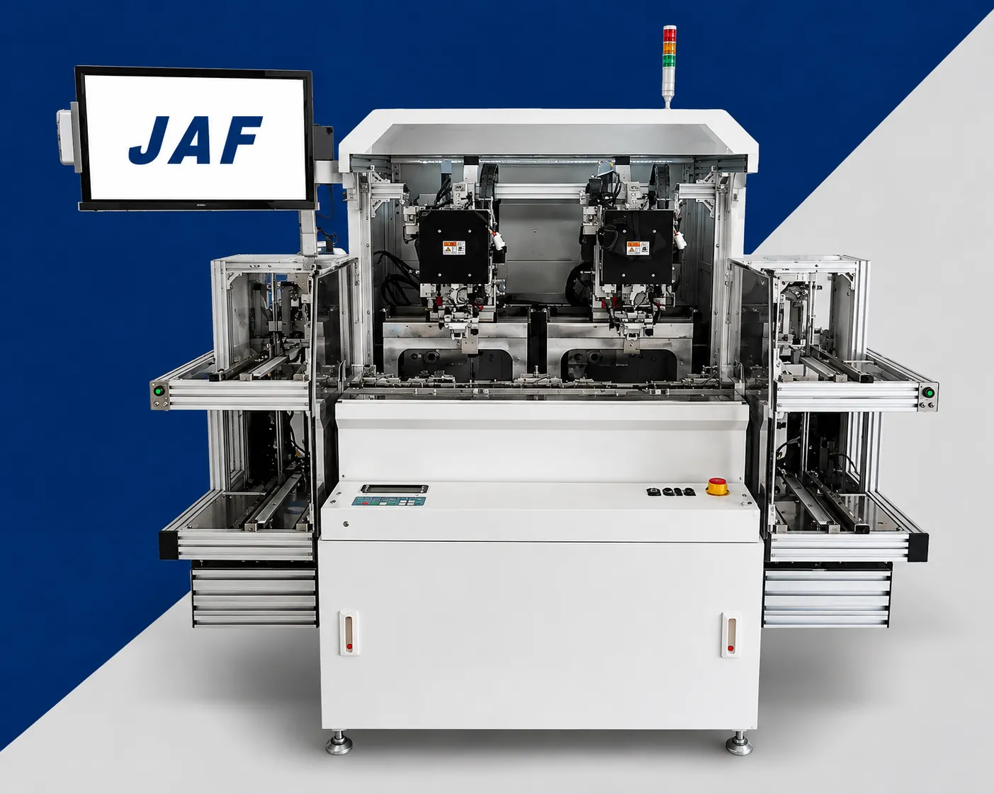
| Applications | Heavy aluminum wire |
| Diameter | 100μm–500μm |
| Materials | Aluminum wire |
| Ultrasonic Frequency | 110KHz |
| Placement Range | X: 130mm Y: 160mm |
| Lead frame size | 100–300mm (L) × 15–65mm (W) × 2mm max. (T) |
| Operation system | Window8, Window10 |
| Waveform Monitoring | Sink, current, voltage, phase, power, VCO |
| Dimensions | L: 1225mm W: 985mm H: 1630mm (Light tower excluded) |
| Die Placement | XY ±2μm @3σ Theta |
| UPH | MAX: 1K |
| Materials – Wafer | Wafer size: 8″, 12″ Die size: 1mm × 1mm ~ 70mm × 70mm Die thickness: 0.05mm ~ 3mm |
| Materials – Boat | Length: 310mm Width: 160mm Thickness: 1mm ~ 5mm |
| Materials – Substrate | Max: 120mm × 120mm |
| Bond force | 3~300N (programmable) |
| Bonding platform | Constant temperature heating, Max: 200°C ±5°C |
| Bond head | Rotation: ±4° Electric leveling, coplanarity <2μm/10mm Pulse heating, 50~450°C, up to 150°C/s |
| Visual | Pre-Bond / Pre Pick, Post-Bond, Uplook |
| Software | Windows OS, graphical human-computer interaction interface, simple and user-friendly. Supports standard SECS/GEM protocols, extends Substrate/Strip/Wafer Mapping E142. Supports Pseudo X-Ray, Post-bond precision detection. |